98.2%
Peak Synchronous Efficiency
TÜV Verified
Factory Direct Onsite Audit
100%
Full Load Burn-In Testing
18+ Years
Power Engineering Heritage
Export Grade Selection
Precision Conversion & Industrial Power Solutions
Engineered for high density, ultra-low thermal dissipation, and rigorous EMI compliance. Explore our factory-direct industrial conversion solutions manufactured in Yueqing, China.
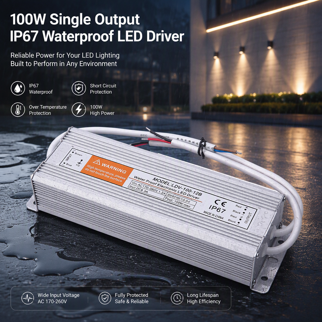
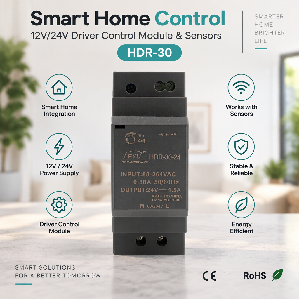
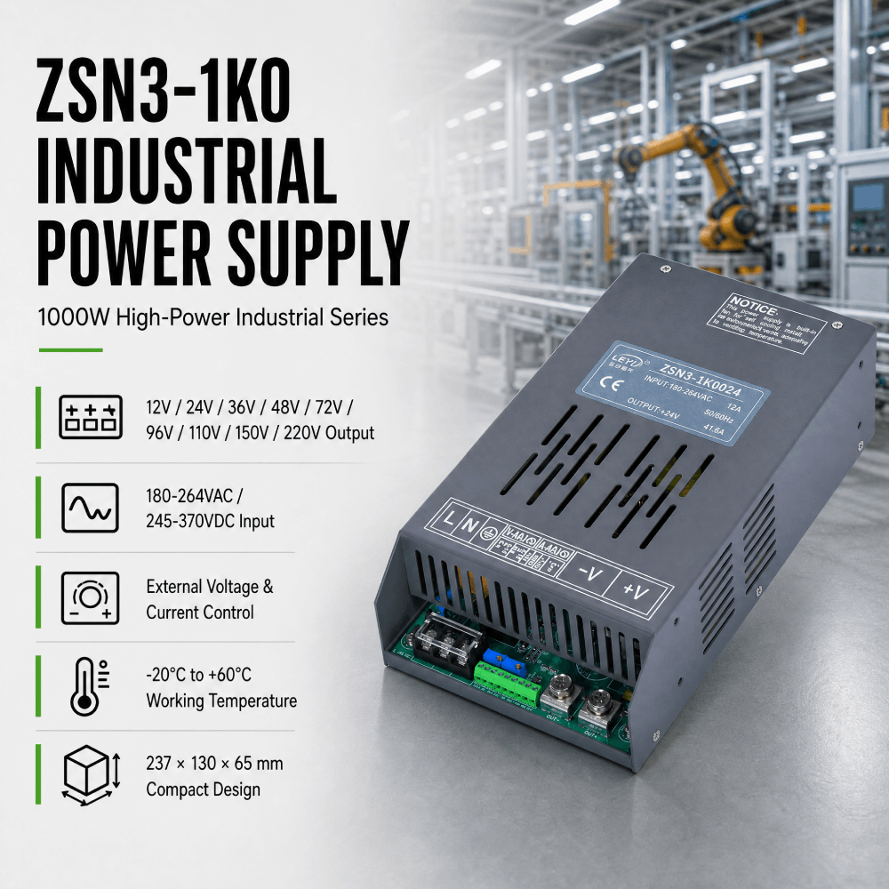
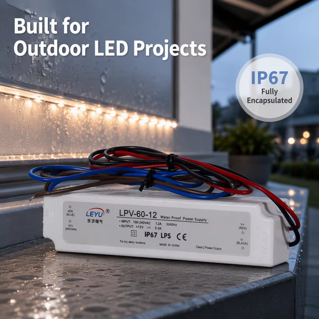
Engineering Deep-Dive
Why Non-Isolated DC DC Converter Topologies Dominate Modern System Architectures
An authoritative analysis of power transfer mechanisms, parasitic inductance mitigation, switching loss physics, and the trade-offs between galvanic isolation and synchronous point-of-load regulation.
Synchronous Rectification Physics
In classical buck conversion topologies, the freewheeling Schottky diode introduces an inevitable forward voltage drop ($V_F \approx 0.4\text{V}-0.7\text{V}$), imposing a severe efficiency ceiling under low-voltage, high-current conditions. Non-isolated synchronous buck converters substitute this diode with an ultra-low $R_{DS(on)}$ N-channel MOSFET driven by complementary gate-timing circuitry.
This structural change drops conduction dissipation from $P_{loss} = I_{out} \times V_F$ to $P_{loss} = I_{out}^2 \times R_{DS(on)}$, enabling conversion efficiencies exceeding 97.5% in compact footprint enclosures.
Elimination of Magnetic Core Saturation
Galvanically isolated converters necessitate intermediate dual-winding planar or toroidal transformers that must endure high volt-second stress and primary-to-secondary dielectric barriers. These transformers are prone to core saturation under dynamic transient steps and inherently introduce significant leakage inductance ($L_{lk}$).
By operating with a single shared common-ground inductive storage element, non-isolated topologies eliminate core loss overheads, transformer fringing flux, and the massive copper volume associated with high-voltage clearance and creepage spacing.
Sub-Nanosecond Transient Response
Feedback control loops across an isolated boundary are forced to transmit error signals through optocouplers or magnetic pulse couplers. Optocouplers display severe bandwidth throttling (<50kHz cutoff), extreme temperature coefficients, and continuous CTR (Current Transfer Ratio) aging degradation over extended operational life.
Non-isolated DC DC converters deploy high-bandwidth direct copper feedback loops (transconductance error amplifiers operating above 500kHz). This architecture enables instantaneous compensation during extreme load slew rates ($dI/dt > 2.5\text{A}/\mu\text{s}$).
| Evaluation Parameter | Non-Isolated Synchronous Converter | Isolated Flyback / Forward Converter | System Impact on OEM Architectures |
|---|---|---|---|
| Typical Conversion Efficiency | 94.0% – 98.5% | 82.0% – 89.5% | Drastically reduced heatsink dimensions and internal cabinet temperature rise. |
| Volumetric Power Density | 180 – 350 W/in³ | 40 – 90 W/in³ | Allows sub-assembly integration directly onto multi-layer motherboards. |
| BOM Cost Structure | Streamlined (No transformer/optocoupler) | Heavy (High-voltage magnetics + isolation barrier) | Achieves 30% to 50% procurement cost reduction at bulk factory export volumes. |
| Ground Plane Structure | Common Ground Reference ($V_{in(-)} \equiv V_{out(-)}$) | Galvanic Break (1500V – 3000V Isolation) | Non-isolated is optimal for single-battery systems, vehicle chassis, and local PoL. |
| Thermal Derating Profile | Extended up to 75°C Ambient | Derates heavily above 50°C Ambient | Guarantees higher MTBF (>500,000 hrs according to Telcordia SR-332). |
Market Intelligence
Emerging Procurement Trends for Global B2B Sourcing Engineers
How Tier-1 industrial buyers, telecommunication infrastructure integrators, and e-mobility designers are transforming DC DC power supply procurement strategies for 2025–2030.
Migration to 48V Distribution Architectures
Industrial automation lines, robotics cells, and hyperscale edge-compute cabinets are migrating from traditional 12V/24V centralized buses to 48V nominal distribution architectures. Operating at 48V reduces $I^2R$ copper distribution losses by a factor of 16 compared to 12V backplanes.
Consequently, procurement requests for high-ratio non-isolated buck step-down modules (48V down to 12V, 5V, or 3.3V) with wide input windows (36V–75V) have surged over 240% across European and North American manufacturing hubs.
GaN & SiC Semiconductor Integration
Wide Bandgap (WBG) materials—specifically Gallium Nitride (GaN) and Silicon Carbide (SiC)—are superseding conventional silicon MOSFETs. GaN's nearly zero reverse recovery charge ($Q_{rr}$) enables conversion switching frequencies to increase from 150kHz to above 1.5MHz.
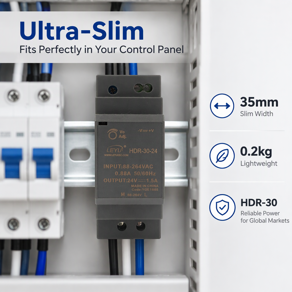
For international sourcing directors, this technological transition delivers extreme miniaturization: passive inductors and filtering capacitors shrink to a fraction of their prior volume, facilitating DIN-rail enclosures that pack twice the wattage in a standard 35mm profile.
Digitally Managed PMBus Telemetry
Purely analog control loops are being paired with or replaced by digital power controllers running PMBus, I2C, or CAN protocols. Factory procurement contracts increasingly stipulate real-time onboard telemetry for voltage trims, operating temperatures, and cumulative current logging.
This allows automated control systems to perform predictive thermal derating and remote power cycle diagnostics without sending technicians into field cabinets.
Manufacturing Excellence
Yueqing Keldan Technology Co., Ltd. — Your Audited China Power Partner
Headquartered in Yueqing, Wenzhou—the globally renowned hub for electrical apparatus manufacturing—Keldan Technology has provided industrial clients with world-class power conversion equipment for more than 18 years.
Our production facilities have been thoroughly checked and onsite-verified by TÜV Rheinland, authenticating our in-house R&D laboratories, automated SMT placement, and strict quality control workflows. We operate not as an opaque trading agency, but as an engineering-driven custom manufacturer supporting OEM/ODM contracts worldwide.
TÜV Rheinland Onsite Verified
100% Full-Load Burn-In Racks
Custom Voltage / Form-Factor ODM
Automated SMT & AOI Inspection
10+ Years International Export Team
CE / RoHS Market Compliance
Procurement Knowledge Base
Frequently Asked Questions on Non-Isolated DC DC Procurement
Clear, direct technical answers to assist hardware design engineers and procurement officers during RFQ evaluation and factory qualification.
What is the fundamental difference between a non-isolated and an isolated DC DC converter?
A non-isolated DC DC converter shares a direct electrical common ground plane between its input and output ($V_{in(-)} \equiv V_{out(-)}$), utilizing an inductor as its energy transfer medium. An isolated converter places an internal high-frequency transformer barrier between input and output, separating grounds and preventing direct electrical continuity (typically rated for 1500V to 3000V dielectric breakdown). Choose non-isolated units when galvanic safety barriers are not required by code, achieving significantly higher efficiency, lower cost, and compact sizing.
When is it safe to specify a non-isolated DC DC converter instead of an isolated model?
Non-isolated converters are ideal when: (1) The input voltage is already derived from a safety-isolated primary power source (such as a certified AC to DC DIN rail supply or battery bank); (2) Both input and output circuits share the same physical chassis or equipment ground; (3) There are no large ground potential differences or high-voltage transient spikes between subsystems; and (4) Strict Point-of-Load (PoL) regulation is required for microcontrollers, sensors, and actuators.
How does Keldan guarantee long-term field reliability and thermal performance?
Every unit produced at our Yueqing factory undergoes an 8-stage quality assurance protocol. This includes on-site incoming inspection of high-grade 105°C Japanese/Taiwanese electrolytic capacitors and automotive-grade MOSFETs, automated pick-and-place SMT, computerized AOI optical verification, manual precision calibration, and 100% full-load thermal burn-in aging on dedicated rack systems before final packaging release.
What custom OEM and ODM specifications can your engineering team accommodate?
With over 5 certified SMPS design engineers, each possessing 5+ years of hands-on power electronics experience, Keldan supports comprehensive design-based and sample-based customization. We develop non-standard input/output voltage ratios (e.g., custom 36V to 7.5V step-downs), customized thermal heatsinks, IP67 waterproof potting, specialized PCB form factors, custom terminal blocks, private labeling, and tailored export packaging.
What are your standard export lead times, MOQs, and sample testing policies?
For standard catalog items, evaluation samples are supported with an MOQ starting from just 1 unit. Production batches typically require minimum order quantities ranging from 10 to 50 units depending on the enclosure and power rating. Standard sample lead times are 3–5 working days, while full container and OEM production shipments generally dispatch within 15–25 business days from our Ningbo or Shanghai export terminals.
Accelerate Your Project with Factory-Direct Power Engineering
Whether you require drop-in replacement non-isolated buck regulators, heavy-duty variable testing supplies, or custom DIN-rail power modules, Keldan Technology delivers audited quality and competitive export pricing directly from the manufacturing source.
Get a Quote